Recently, the Institute of Microelectronics of the Chinese Academy of Sciences has made progress in the integration of resistive memory and large-scale production CMOS processes.
Resistance variable memory (RRAM) is a new type of non-volatile memory technology that has emerged in recent years. It has the advantages of small cell size, fast speed, low power consumption, simple process and device structure and strong embeddable functions. It is an internationally recognized 32nm node One of the strong competitors of the following mainstream memory technologies. The RRAM team led by Researcher Liu Ming from the Nano-Processing and New Device Integration Technology Laboratory of the Institute of Microelectronics (Room 3) has carried out many years of research in this field, based on binary metal oxide materials compatible with CMOS processes , Mechanism research, scalability research, reliability research, small array prototype chip design, test methodology research and other aspects have achieved a domestic leading position and a series of internationally influential results.
In 2012, supported by the National Science and Technology Major Project "32nm RRAM Key Process and Technology", the RRAM R & D team completed the tape-out work of RRAM peripheral circuits on the SMIC production line, and successfully developed a 1kb RRAM array and Integrated process of peripheral circuit chips. On the one hand, this integrated solution adopts a large-scale production platform to provide early technical reserves for the company's production research and development; on the other hand, taking into account the flexible and diverse characteristics of the laboratory, it can be free from the restrictions of the types of materials on the CMOS process. The research of the new structure device has laid a good foundation for the further development of the cooperation mode of industry, university and research institute.
The research achievements of the scientific research team have also received widespread attention from international peers, and signed cooperative development agreements with VSEA and Adesto in the United States, respectively.

Left: (a) RRAM storage array test system; (b) machine-level test pin card physical map; (c) PCB board control circuit part.
Right: (a) The physical map of the RRAM 1kb chip under the probe card; (b) The bitmap of the word "IME" written in the array.
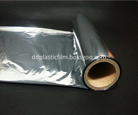
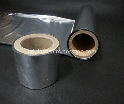
Raw materisl :Metallized BOPA film , Metallized Nylon/PE composite film and other High Barrier Film
Thickness: 15mic, 18mic, 24mic ect. Accept customized
Application : Making ballon, For high barrier packaging
Characteristics
1.Excellent resistance to puncture and abrasion.
2.Good barrier against oxygen, nitrogen, carbon dioxide and odor.
3.Resistant to acid, alkaline, grease and different kinds of common organic solvent.
4. High transparency and gloss and metallized high barrier.


Nano Coating Metallized Film
Multi-Layer Metallic film,Metalized Bopa Film,Metallized Nylon Film,Nano Coating Metallized Film
Shijiazhuang dadao Packaging materials Co , https://www.ddplasticfilm.com